- 您现在的位置:买卖IC网 > Sheet目录514 > SIHG20N50C-E3 (Vishay Siliconix)MOSFET N-CH 500V 20A TO247
SiHG20N50C
Vishay Siliconix
Power MOSFET
PRODUCT SUMMARY
FEATURES
? Halogen-free According to IEC 61249-2-21
V DS (V) at T J max.
560
Definition
R DS(on) ( Ω )
Q g (Max.) (nC)
Q gs (nC)
Q gd (nC)
Configuration
V GS = 10 V
76
21
34
Single
D
0.270
? Low Figure-of-Merit R on x Q g
? 100 % Avalanche Tested
? High Peak Current Capability
? dV/dt Ruggedness
? Improved T rr /Q rr
? Improved Gate Charge
? High Power Dissipations Capability
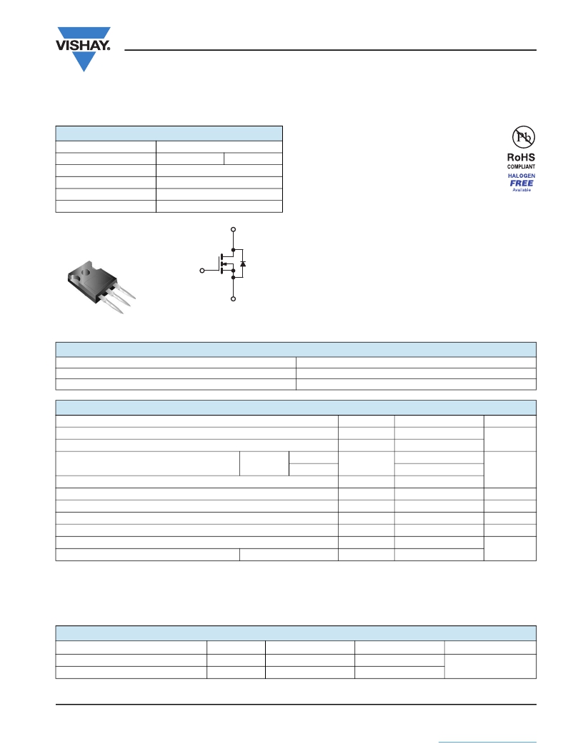
TO-247AC
G
? Compliant to RoHS Directive 2002/95/EC
D
S
S
G
N-Channel MOSFET
ORDERING INFORMATION
Package
Lead (Pb)-free
Lead (Pb)-free and Halogen-free
TO-247AC
SiHG20N50C-E3
SiHG20N50C-GE3
ABSOLUTE MAXIMUM RATINGS (T C = 25 °C, unless otherwise noted)
PARAMETER
Drain-Source Voltage
Gate-Source Voltage
SYMBOL
V DS
V GS
LIMIT
500
± 30
UNIT
V
Continuous Drain Current (T J = 150 °C) e
Current a
Pulsed Drain
V GS at 10 V
T C = 25 °C
T C = 100 °C
I D
I DM
20
11
80
A
Linear Derating Factor
1.8
W/°C
Single Pulse Avalanche Energy b
Maximum Power Dissipation
Peak Diode Recovery dV/dt c
E AS
P D
dV/dt
361
250
5
mJ
W
V/ns
Operating Junction and Storage Temperature Range
Soldering Recommendations (Peak Temperature)
for 10 s
T J , T stg
- 55 to + 150
300 d
°C
Notes
a. Repetitive rating; pulse width limited by maximum junction temperature.
b. V DD = 50 V, starting T J = 25 °C, L = 2.5 mH, R g = 25 Ω , I AS = 17 A.
c. I SD ≤ 18 A, dI/dt ≤ 380 A/μs, V DD ≤ V DS , T J ≤ 150 °C.
d. 1.6 mm from case.
e. Limited by maximum junction temperature.
THERMAL RESISTANCE RATINGS
PARAMETER
Maximum Junction-to-Ambient
Maximum Junction-to-Case (Drain)
SYMBOL
R thJA
R thJC
TYP.
-
-
MAX.
40
0.5
UNIT
°C/W
Document Number: 91382
S11-0440-Rev. C, 14-Mar-11
www.vishay.com
1
This datasheet is subject to change without notice.
THE PRODUCT DESCRIBED HEREIN AND THIS DATASHEET ARE SUBJECT TO SPECIFIC DISCLAIMERS, SET FORTH AT www.vishay.com/doc?91000
发布紧急采购,3分钟左右您将得到回复。
相关PDF资料
SIHG24N65E-E3
MOSFET N-CH 650V 24A TO247AC
SIHP12N60E-E3
MOSFET N-CH 600V 12A TO220AB
SIHP30N60E-E3
MOSFET N-CH 600V 29A TO220AB
SIHP5N50D-E3
MOSFET N-CH 500V 5.3A TO220AB
SIHP6N40D-E3
MOSFET N-CH 400V 6A TO-220AB
SIHP7N60E-GE3
MOSFET N CH 600V 7A TO-220AB
SIHU3N50D-E3
MOSFET N-CH 500V 3A TO251 IPAK
SIHU5N50D-E3
MOSFET N-CH 500V 5.3A TO251 IPAK
相关代理商/技术参数
SIHG22N50D-E3
功能描述:MOSFET 500V 22A 312W 230mOhm @ 10V
RoHS:否 制造商:STMicroelectronics 晶体管极性:N-Channel 汲极/源极击穿电压:650 V 闸/源击穿电压:25 V 漏极连续电流:130 A 电阻汲极/源极 RDS(导通):0.014 Ohms 配置:Single 最大工作温度: 安装风格:Through Hole 封装 / 箱体:Max247 封装:Tube
SIHG22N50D-GE3
功能描述:MOSFET 500V 230mOhm@10V 22A N-Ch D-SRS
RoHS:否 制造商:STMicroelectronics 晶体管极性:N-Channel 汲极/源极击穿电压:650 V 闸/源击穿电压:25 V 漏极连续电流:130 A 电阻汲极/源极 RDS(导通):0.014 Ohms 配置:Single 最大工作温度: 安装风格:Through Hole 封装 / 箱体:Max247 封装:Tube
SIHG22N60E
制造商:VISHAY 制造商全称:Vishay Siliconix 功能描述:E Series Power MOSFET
SIHG22N60E_13
制造商:VISHAY 制造商全称:Vishay Siliconix 功能描述:E Series Power MOSFET
SiHG22N60E-E3
功能描述:MOSFET 600V 180mOhm@10V 21A N-Ch E-SRS
RoHS:否 制造商:STMicroelectronics 晶体管极性:N-Channel 汲极/源极击穿电压:650 V 闸/源击穿电压:25 V 漏极连续电流:130 A 电阻汲极/源极 RDS(导通):0.014 Ohms 配置:Single 最大工作温度: 安装风格:Through Hole 封装 / 箱体:Max247 封装:Tube
SIHG22N60E-GE3
功能描述:MOSFET 600V 180mOhm@10V 21A N-Ch E-SRS
RoHS:否 制造商:STMicroelectronics 晶体管极性:N-Channel 汲极/源极击穿电压:650 V 闸/源击穿电压:25 V 漏极连续电流:130 A 电阻汲极/源极 RDS(导通):0.014 Ohms 配置:Single 最大工作温度: 安装风格:Through Hole 封装 / 箱体:Max247 封装:Tube
SIHG22N60E-GE3
制造商:Vishay Siliconix 功能描述:MOSFET N CH 600V 21A TO-247AC-3
SiHG22N60S
制造商:Vishay Semiconductors 功能描述:
